
Semiconductors are essential for creating modern electronic devices. Due to this critical role, the global semiconductor industry is both extensive and competitive. It’s projected to grow 6%-8% through 2030, with annual revenues predicted to reach $1 trillion.1
The semiconductor manufacturing process is a complex journey requiring several intricate, time-consuming steps, and it’s constantly evolving with the introduction of new technologies. Learn how semiconductors are made in this comprehensive guide.
An Overview of Semiconductors and Their Applications
Any material that has features of both conductors and insulators — but doesn’t fall into either classification — is considered a semiconductor. Semiconductors can be pure elements, such as germanium and silicon.2 Alternatively, they can be compounds like gallium arsenide (GaAs) and cadmium selenide (CdSe).
Semiconductors are a vital component in electronic devices across several sectors, such as health care, communications, military, transportation and energy. They have multiple technology applications, including diodes, transistors, microprocessors, solar cells and LED lights.3 Manufacturers often use semiconductors for various devices that rely on electricity, such as:
- CPUs.
- Mobile phones.
- Televisions.
- Digital cameras.
- Radios.
- Diagnostic imaging equipment.
The Semiconductor Manufacturing Process
Semiconductor manufacturing processes are highly elaborate, involving extreme precision and specialized materials and equipment. The entire process can take anywhere from a few weeks to several months, depending on the chip’s complexity and the technology being used.
Many of these steps contain a variety of precise subprocesses. Additionally, the manufacturer may repeat the entire sequence to increase the chip’s complexity and the number of transistors. By the time they complete the following steps, there may be up to billions of transistors on semiconductor chips:
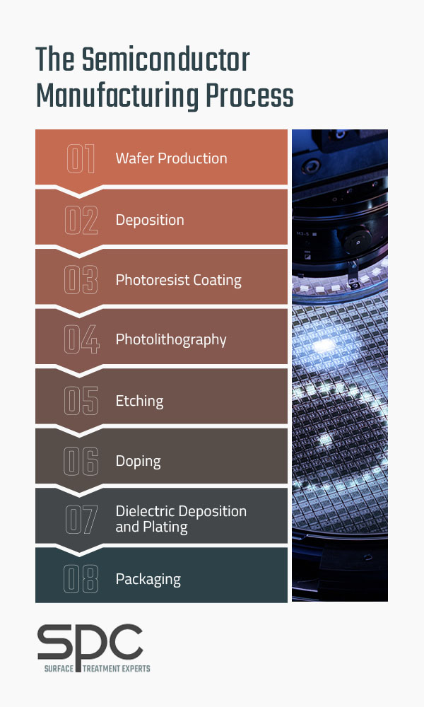
1. Wafer Production
A semiconductor typically begins as a smooth, wafer-thin slice of a purified material.4 Manufacturers create these wafers by heating, molding, processing and cutting the material. Wafers can vary in size, each containing dozens or even thousands of chips.
First, carbon is heated with silicon dioxide to create a bar of pure silicon, also known as an “ingot.” Wafers are sliced from the ingot and polished for optimal smoothness, creating the basis of the semiconductor chip. The wafers are cleaned, heated and exposed to pure oxygen using a diffusion furnace. This process creates a uniform film of silicon dioxide on the wafer’s surface.
2. Deposition
Next, the manufacturer deposits thin films of conducting, semiconducting or isolating materials — depending on the product being made — onto the wafer so they can print the first layer on it. This process, known as “deposition,” is used to create electronic components. It can be accomplished with a range of techniques, such as:
- Chemical vapor deposition (CVD): CVD involves depositing a solid material from a vapor using a chemical reaction occurring in or near a heated substrate surface.5 The resulting solid material takes the form of a thin film.
- Physical vapor deposition (PVD): PVD consists of three main steps — vaporizing a solid material, transporting the disintegrated material and nucleating it to create nanoparticles and thin films.6
- Atomic layer deposition (ALD): ALD is a special variant of the CVD technique that introduces gaseous reactants, or precursors, to a reaction chamber to create the desired material using chemical surface reactions.7 These precursors are pulsed one at a time and separated using inert gas purging to prevent gas phase reactions. This process enables controlled growth of the desired material and a uniform film.
Manufacturers can use these processes to deposit materials like metals, nitrides and oxides.
3. Photoresist Coating
The manufacturer then applies the wafer with photoresist, a light-sensitive coating. Two types of photoresist exist:8
- Positive: The primary difference between positive and negative photoresist is the material’s chemical structure and how it reacts with light. In a positive photoresist, the areas exposed to ultraviolet light become more soluble, preparing them for etching. Positive photoresist is more prevalent in semiconductor manufacturing, as its high resolution makes it ideal for photolithography.
- Negative: In negative photoresists, the exposed areas polymerize, making them stronger and insoluble.
4. Photolithography
Also called “photo-masking,” photolithography is an important step in the semiconductor chip manufacturing process. It creates a pattern on the silicon wafer.
After coating one part of the wafer with a light-sensitive film, the manufacturer inserts the chip wafer into a lithography machine, exposing the material to deep or extreme ultraviolet light through a mask.9 The mask contains a pattern that corresponds to the electronic component being manufactured. Photolithography exposes the film to the mask pattern, protecting one area of the wafer while the manufacturer works on another.
The system’s optics shrink and focus the pattern onto the photoresist layer. When light hits the photoresist, it sparks a chemical change that allows the pattern to be replicated onto the photoresist layer. The manufacturer then removes the areas of the light-exposed photoresist, leaving behind a patterned surface on the wafer.
Achieving the precise pattern can be challenging, as chemical and physical defects like particle interference and refraction can occur. Sometimes, the manufacturer may need to intentionally deform the blueprint to optimize the pattern.
5. Etching
Next, the manufacturer removes the degraded photoresist to reveal the desired pattern. A process called “etching” is used to bake and develop the wafer, harden the remaining film pattern and expose it to a chemical solution to remove areas not covered by the hardened film. The manufacturer removes the film and inspects the wafer to ensure effective image transfer.
Similar to photoresist coatings, there are multiple types of etching techniques:10
- Wet: Wet etching washes the wafer in a bath of chemical liquids to transfer a pattern to the material.
- Dry: Dry etching transfers a pattern to a material using reactive gases to define the exposed pattern on the wafer. This technique is usually more complex than wet etching, and a drawback is that it may lack selectivity between different materials. However, a benefit of dry etching is that it is anisotropic, allowing for replicable etch characteristics.
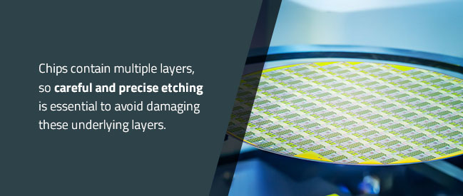
The etching process should consistently and accurately create conductive features without compromising the chip’s overall structural integrity and stability. Chips contain multiple layers, so careful and precise etching is essential to avoid damaging these underlying layers.
Advanced etching technology allows chip manufacturers to use double, quadruple and spacer-based patterning to develop the tiny, intricate features prominent in modern chip designs — all without damaging the chip’s structure.
6. Doping
After etching patterns into the wafer, the manufacturer may bombard the wafer with positive or negative ions to enhance the material’s electrical conductivity.
During the doping stage, the manufacturer adds impurities to the silicon wafer to alter its electrical properties. The most commonly used impurities are phosphorus and boron, which are added in small traces to create p-type and n-type semiconductors.11
Adding atoms with one more electron than the material is called n-type doping, as it adds a free electron to the silicon lattice to give the material a negative. Conversely, p-type doping adds atoms with one less electron. It creates holes in the silicon lattice where a silicon electron has nothing to bond to, generating a positive charge.
Raw silicon isn’t an inherently strong conductor or insulator — its electrical properties fall somewhere in the middle. Both doping methods can convert the semiconductor into a strong conductor.
The manufacturer adds these impurities using a process called ion implantation, where ions are accelerated to high speeds and implanted into the wafer’s surface.12 Directing electrically charged ions into the silicon enables a more controlled flow of electricity and helps create transistors — electronic switches that serve as the basic building blocks of microchips.
After implanting the ions, the manufacturer removes the remaining sections of photoresist that protected areas of the wafer not intended to be modified.
7. Dielectric Deposition and Plating
The manufacturer connects the devices by adding layers of metals and insulators. As one of the final steps of the semiconductor manufacturing process, plating helps protect the circuits and create a connection between the semiconductor’s internal components and the outside world.
The manufacturer adds a final insulating layer to safeguard the circuit against contamination and damage. They also etch openings into the film to enable access to the top metal plate.
Manufacturers often use electroplating or electrodeposition to plate semiconductors.13 This process applies a thin metal layer onto the substrate and typically involves the following steps:
- The plating metal is connected to the electrical circuit’s positively charged electrode, or anode.
- The substrate is placed at the negatively charged electrode, or cathode.
- The substrate and metal coating are immersed in an electrolytic solution containing one or more metal salts to boost electricity flow.
- A DC is added to the circuit using a power source, applying a current to the anode and introducing electricity to the system.
While these are the general steps for electroplating, plating a semiconductor is a smaller-scale process than standard electroplating projects. Semiconductor chips range in size, though several companies are working toward smaller node sizes than are currently available today.14
The circuits within these chips contain microscopic wires. With that in mind, any flaws in the semiconductor — such as breakage or the entrance of dust particles — can easily damage the final product. That’s why manufacturers must take extra precautions to ensure a quality finished product.
8. Packaging
At this point, the chip is ready to be tested, packaged and assembled so it can be mounted on a printed circuit board (PCB) and integrated into a product.
During this final phase, the manufacturer packages the electronic components into a finished product, which can be used in electronic devices. This process involves cutting wafers down to individual chips, attaching them to a substrate, like a PCB, and connecting them to other components via wires to direct input and output signals.
To complete the packaging process, a heat spreader — a small, flat metal container with a cooling solution — is placed over the chip to protect the fragile component and dissipate heat buildup, keeping the microchip cool during operation.
What Materials Are Used to Plate Semiconductors?
Some common metals for electroplating semiconductors include:15
- Gold: Gold is highly conductive and heat-resistant.16 It’s often applied on top of nickel, which provides a protective barrier against corrosion by preventing rust from entering through pores on the gold’s surface.
- Silver: Silver offers excellent electrical and thermal conductivity.17 It’s also compatible with various metals. Due to its high solderability and low contact resistance, silver is often used to coat copper parts.
- Tin and tin alloys: Tin is a cost-effective alternative to more expensive materials like gold, silver, and platinum.18 This material offers good contact resistance, corrosion protection, and solderability. However, it is less conductive than other metals and can form sharp protrusions called “whiskers” that can damage surrounding materials. Tin alloys may be used to minimize whiskers. Plus, unlike pure tin, they often don’t require undercoating.
- Copper: Copper is prized for its electrical and thermal conductivity, corrosion resistance and malleability, making it a popular plating material in the electronics industry.19 While effective on its own, copper may be reinforced with an additional metal coating to further enhance this performance.
- Nickel: Nickel provides impressive corrosion resistance, as the electroplating process creates a less porous microcrystalline structure as a protective barrier for the substrate.20 When alloyed with other metals, such as tungsten, tin, palladium or zinc, nickel is highly wear-resistant, solderable and electrically conductive.
Navigating Challenges in Semiconductor Manufacturing
Semiconductor production is a significant investment in time and money. Manufacturers face several other roadblocks along the way, from production costs to demand fluctuations and talent shortages. However, the industry also presents opportunities for growth and innovation when addressing these obstacles.
1. Demand
Semiconductor demand is constantly growing, and meeting this demand requires the efficient delivery of critical systems and components and ongoing communication between manufacturers and suppliers.
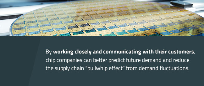
Rapidly evolving technology often requires semiconductor manufacturers to adjust their supply chains accordingly. In many cases, communication between supply chain parties — including fabricators, vendors, equipment manufacturers and testers — is weak or comes too late in the project. By working closely and communicating with their customers, chip companies can better predict future demand and reduce the supply chain “bullwhip effect” from demand fluctuations.
2. Limited Talent
In the United States, the large-scale construction of semiconductor fabrication plants hasn’t occurred in over 20 years.21 Few builders possess the expertise and capabilities needed for these specialized projects.
To exacerbate this issue, semiconductor manufacturers must compete with organizations across various industries in a tight labor market. As more fabrication plants are completed, they’ll also face competition for technical personnel required to operate them.
3. Emphasis on Sustainability
Sustainability is becoming a higher priority for semiconductor manufacturers, as many of their customers want to reduce their supply chain emissions. A study showed that only about 60 of 2,000 companies have committed to emissions targets, and many semiconductor companies lack clearly defined sustainability goals.22 Semiconductor production is responsible for high emissions associated with finished products, causing the industry to face scrutiny from end customers.
As more end customers place value on net-zero emissions, semiconductor companies are searching for ways to achieve actionable emissions targets. For example, semiconductor fabrication plant owners could benefit from investing in renewable energy resources when building new locations.
4. Cost and Inventory Challenges
With production costs on the rise23 — and companies still recovering from the global semiconductor chip shortage of 2022 — many organizations must employ leaner manufacturing practices.24 That often means purchasing later and keeping buffer inventory low. Manufacturers must find a middle ground between inventory stockpiling and timely production.

Contact SPC for Your Electronics Plating Needs
Plating semiconductors, connectors and other electronic components is a challenging process requiring extreme precision and expertise. At SPC, we have over 90 years of metal finishing experience under our belt.25
Our experts can help you select the best electronics plating and metal finishing processes for your unique applications. We serve companies across numerous industries, and we strive for the most eco-conscious plating solutions.26
Call 717-767-6702 for more information about our services, or submit a quote form today.27
Endnotes:
- https://www.mckinsey.com/industries/industrials-and-electronics/our-insights/semiconductor-fabs-construction-challenges-in-the-united-states
- https://www.semiconductors.org/semiconductors-101/what-is-a-semiconductor/
- https://irds.ieee.org/topics/new-semiconductor-technologies-and-applications
- https://www.sharrettsplating.com/industries/plating-semiconductors
- https://www.sciencedirect.com/topics/materials-science/chemical-vapor-deposition
- https://www.sciencedirect.com/topics/engineering/physical-vapor-deposition
- https://www.sciencedirect.com/topics/engineering/atomic-layer-deposition
- https://www.halbleiter.org/en/photolithography/resist/
- https://www.sciencedirect.com/topics/physics-and-astronomy/photolithography
- https://www.mri.psu.edu/nanofabrication-lab/capabilities/etching
- https://www.halbleiter.org/en/fundamentals/doping/
- https://www.sciencedirect.com/topics/chemistry/ion-implantation
- https://www.sharrettsplating.com/blog/what-electroplating/
- https://spectrum.ieee.org/a-better-way-to-measure-progress-in-semiconductors
- https://www.sharrettsplating.com/coatings/
- https://www.sharrettsplating.com/coatings/gold
- https://www.sharrettsplating.com/coatings/silver
- https://www.sharrettsplating.com/coatings/tin
- https://www.sharrettsplating.com/coatings/copper
- https://www.sharrettsplating.com/coatings/nickel
- https://www.mckinsey.com/industries/industrials-and-electronics/our-insights/semiconductor-fabs-construction-challenges-in-the-united-states
- https://www.mckinsey.com/industries/industrials-and-electronics/our-insights/semiconductor-fabs-construction-challenges-in-the-united-states
- https://www.bls.gov/mxp/publications/industry-pamphlets/semiconductor-industry-facts.htm
- https://www.semiconductors.org/the-state-of-the-industry-report-highlights-challenges-and-opportunities-facing-u-s-chip-industry/
- https://www.sharrettsplating.com/industries/electronics-electroplating
- https://www.sharrettsplating.com/about/environmentally-friendly
- https://www.sharrettsplating.com/quotes/
