Written By Igor Kadija
CET is a novel electroplating technology. It enables design and introduction of advanced electroplating equipment and products. With a unique approach to interaction between the electrical contact and electric field it expands the electroplating technique to currently unimaginable levels.
Exploring the Fundamentals of Contactless Electroplating Technology
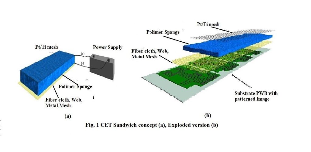
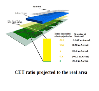
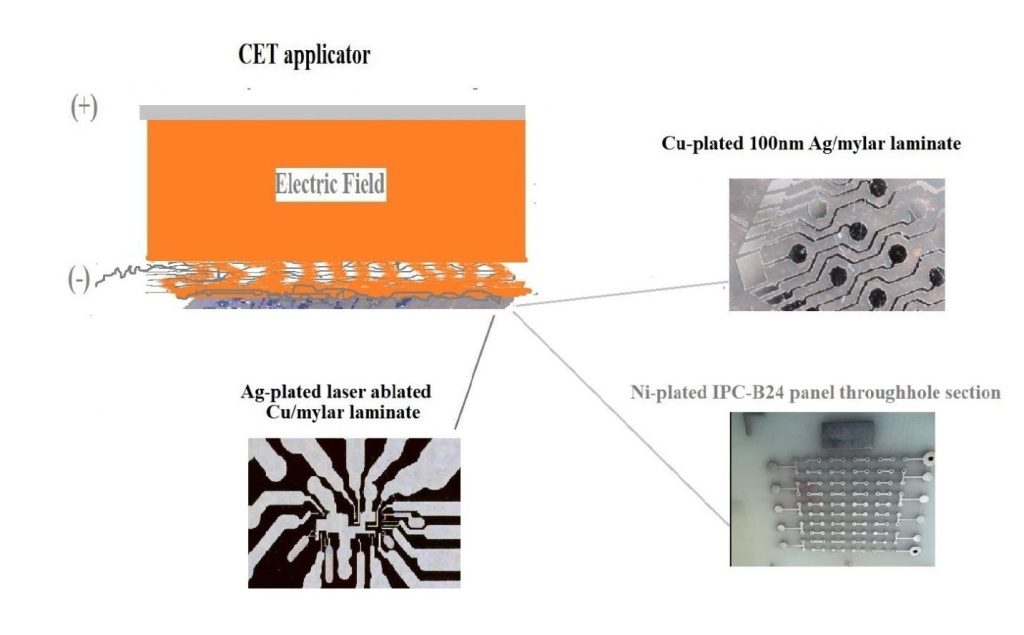
CET is a sandwich, Fig. 1, composed of two thin, porose, flexible conductive blankets with an electrolyte-soaked sponge between them. The positive pole of the power supply is attached to the positive, anode, blanket side. The anode can be an insoluble Pt/Ti mash or a perforated metal to provide replenishments for plated out metal on the cathode side of the cell. The CET cathode blanket, having electrical contacts in the range from 10,000 -50 million/in2 is attached to the negative pole of the power supply. While operating, the negative side of the CET cell is contacting the substrate and reciprocating with programmed frequency and pressure.
Distinctive Advantages Over Traditional Electroplating Methods
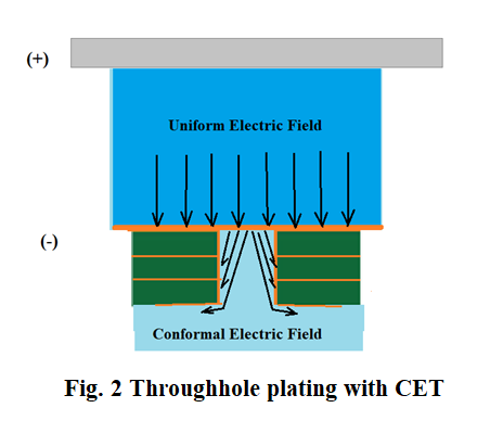
The operator does not have to be concerned with edge effects and throughholes handling. The electroplating cell is defined with two blanket electrodes without distinct features such as interconnects, pads and throughholes, Fig. 2. Within the cell, the two blanket contacts encompass the electroplating process there. Both sides are having a two-dimensional plane with contacts randomly distributed across the surface. To that point the entire electric field within the cell is extremely uniform.
The actual electroplating of substrates starts beyond the CET cathode blanket. The contact is fixed and plating proceeds with electric field being present across the entire metal patterns including throughholes, Fig. 2.
The Mechanisms Powering Contactless Electroplating
The Pivotal Role of Electric Fields in Achieving Contactless Deposition
On the opposite side of the cathode blanket the plating of the substrate proceeds with direct contact to the patterns. From that point on the entire pattern is shorted out via CET cathode. The plating proceeds with electric field propagation through the electrolyte. One can interpret the phenomenon because of a weak Faraday cage. Regardless of the metal permeated CET cathode, the electric field penetrates with the electrolyte through the blanket. From that point on there are no secondary electric fields. The only requirement is to have electrolyte penetration including the throughholes. As the electrolyte is flooding the substrate the electroplating proceeds with electric field spreading with deposit. The electroplating of both the blanket and the substrate proceeds with the nominal rate calculated for the projected surface area of the CET cathode blanket. As a result, the CET blanket can be electroplated with currents larger than nominal plating rate relative to their surface, when single wires contact the substrate pattern, see Fig. 3.
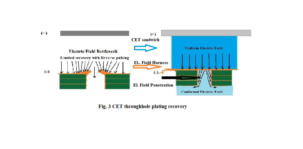
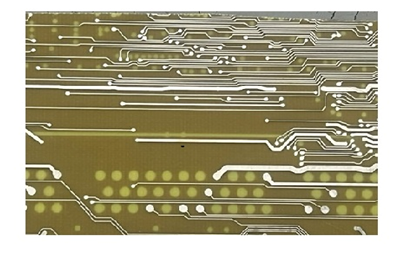
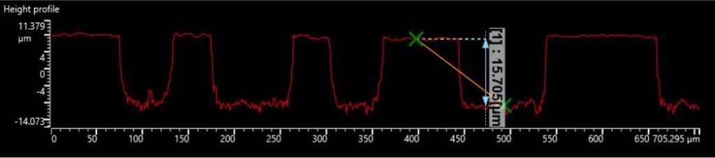
While the substrate is electroplated as needed the single wire may be plated beyond acceptable level. On the contrary, when contacting the substrate with millions of contacts per square inch, the surface area of contacts is orders of magnitude larger than the contacted pattern. The resulting plating of the contacts is orders of magnitude smaller than the substrate, see Fig. 4. Clearly, selection of CET cathode depends on the substrate design. The cumulative effect of repeated plating application determines the maintenance time for replacement and cathode recovery.
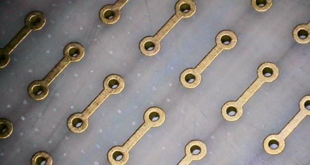
Fig. 4 CET smooth throughholes transition
Why Eliminating Physical Contact Revolutionizes The Electroplating Process
Conventional process calls for individual electrical contact to all parts of a pattern, including the variety of processes such as surface finishing and throughholes. Plating racks, conductive tapes, seed layers, electroless plating, immersion plating, laser processing, ink printing etc. make it possible to produce advanced products at significant labor, material, and equipment cost. By establishing single contact throughout the substrate pattern the CET blanket eliminates the need for individual contacts. The interconnects, pads, throughholes and surface finish can be completed by applying CET in a conveyorized system.
Unveiling the Benefits of CET
Attaining Unparalleled Precision and Uniformity in Metal Deposition
All patterns on the substrate are in a two-dimensional plane, with throughholes. Including the multiple cathode blanket contacts, they are all plated at the preferred current density rate per unit surface area. For example, for a 100 mm x200 mm CET cathode the 6 A total current applied to the CET is calculated based on the assumption that the entire projected surface of the blanket is Ni plated at the desired current density. Increasing the total current to 24 A increases the throughput but the ratio of the substrate vs total remains the same. The actual electroplatable area of the substrate is only a well-defined fraction two-dimensional electroplated surface. As such it is extremely uniform.
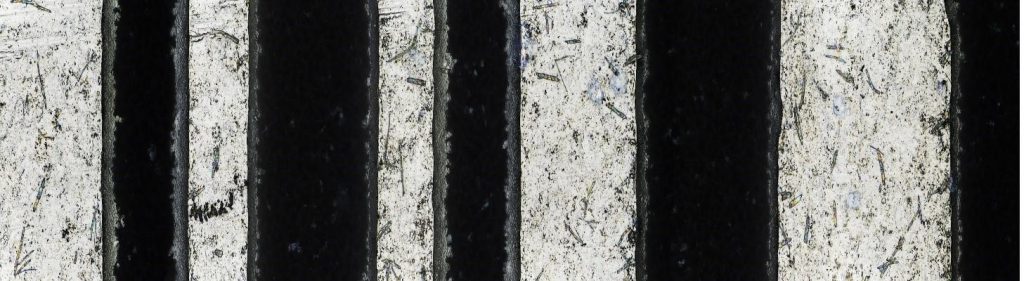
It is worth noting, the CET plating is taking place across the entire plateable surface regardless of the pattern features. Electronics designers purposely develop designs that may avoid sharp edges although these may offer preferential space utilization and signal speed propagation. Eliminated. Secondly, the ubiquitous dog-boning formed at the through hole entrances, see Fig. 3, is cured with extensive surface preparation such as offered by IBE Electronics. Eliminated. The Colloidal Graphite Process by Technic can be applied in a conveyor operation by utilizing superior CET process control. Consequently, the uniformity and processing ease is exceptional.
Significant Reductions in Waste and Environmental Footprint
Let us consider the footprint and the magnitude of a conveyorized CET system for comparison to the conventional processing of PWBs. Conventional processing like reel-to-reel and electroplating tank processing requires electrical contact distribution and handling, plating tanks, racks lifters, surface finishing processing, throughholes processing, rinsing stations etc. The CET system itself needs a significantly smaller footprint and less associated processing sections. Instead of electroless plating and immersion plating and throughholes processing the material flow through the process is continuous. Separate electroless and immersion chemistries and processing are eliminated, the waste and environmental impact minimized.
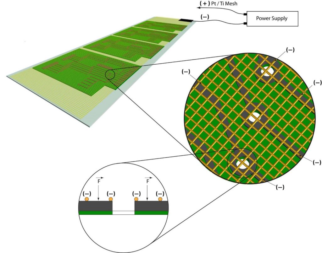
CET electric contact and electric field access to substrate
Elevating Worker Safety to New Heights
By elimination of extra processing steps such as contact introduction, electroless, immersion and through hole processing CET enables less maintenance, less operator travel, less chemical spillage possibilities. By removing specialty chemicals such as electroless and immersion application the facility can reduce its expenses and improve the operators safety.
CET’s Impact Across Industries
Revolutionizing Aerospace and Automotive Manufacturing
Aerospace and automotive manufacturing electronics need to excel and exceed the standards for heat and vibration reliability. The current standards are based on available manufacturing capabilities that barely meet the needs. NASA and DOD have special requirements to avoid failures in thermal and vibrational conditions. CET has already demonstrated the capability to recover failing devices with current surface finishes such as ENIG.
Pioneering Applications in Electronics and Circuit Board Production
CET makes a pivotal step in pioneering applications in electronics and circuit board production. Advanced computing such as supercomputers and quantum computing devices, 2D, 3D and plus PCBs all require HDIs capable of meeting the need for micro and nanosize interconnects and pads. CET concept is applicable of delivering micro and nanosize features with appropriate lithography.
Breakthroughs in the Medical Device Sector
One can bring up the two major examples of medical devices needing precision micro and nano size electroformed features. Various implants can be produced with CET application. Microscopic spirals can be used as antennae for emitting signals from the body to the outside world. An example of this was demonstrated with microscopic soccer player back in 2007 produced by IRIS group in Zurich ETH Switzerland.
Compatibility and Flexibility of CET
Identifying Compatible Materials for CET Application
CET processing has a broad range of applicability. In general, any conductive pattern, flexible or rigid, having resistance less than 1000 kiloohmscm2 and adhering with good tape test is an acceptable candidate. For example, nanosize metal/mylar laminates, conductive ink patterns, metal monolayer patterns, DBC and other ceramic substrates are acceptable candidates for CET application.
CET plated etching test pattern with 3 micron Ni plating over ½ mil etched laminate
Exploring the Wide Array of Metals Suitable for CET Deposition
Most metal and alloy electroplating solutions such as Cu, Ni, Ag, Au, Pd, Sn are suitable for CET deposition. CET is a preferable method for deposition of alloys. It maintains the appropriate composition of components at the very interface enabling optimal deposit ratio.
Evaluating the Cost Benefits of CET
Analyzing Cost Comparisons with Traditional Plating Methods
According to researchandmarket.com, the Global PCB Market is expected to reach an estimated $89.7 Billion by 2024: IC Substrate, Rigid, 2-Sided, Multilayer, Rigid Flex, laminate material, and others.
Industry has sought and established methods to bypass the need for direct contact with the power supply. However, the majority of these methods do not include electroplating as a most desirable option. Currently, conveyor-based method known as coil-to-coil or roll-to-roll processing has made a step forward in electroplating application. By upgrading the same with CET it would eliminate the exposure of the pattern to the electric field and throughholes processing facing the inside of the cell. In addition, it would increase the plating rate by 2-3 times by increasing plating current density. That would enable the conveyor line speed up to 10 to 30 feet per minute. No other methods like electroless, inkjet, e-jet, screen printing, metal paste, sputtering, vapor deposition, and others come even close to the 99% level achievable by electrodeposition. In addition, CET enables control of the process in conformity and uniformity of deposits far beyond the state-of-the-art technologies.
It is estimated that the cost of ENIG and/or ENEPIG surface finish or Ni and Au plating in a reel-to-reel process still reaches up to 15% of the production cost, cutting off the profit for the manufacturer. Labor Cost competitiveness becomes an issue when the current standards impose excessive processing in the absence of the adequate electroplating processes proposed with CET.
Highlighting The Long-Term Economic Advantages for Businesses
For comparison, implementation of the CET achieves both a production cost reduction of over 25% while improving the quality and competitiveness in the market world. Isolated Patterns Electroplating, Surface Finishing Optimization, Chemical Hazard Elimination, Throughholes Plating and Electric Field Harnessing will become the new standard in Electronics.
Quality Assurance: CET vs. Traditional Electroplating
Both, the simplicity of the material flowchart and resulting quality of products with CET are superior to conventional techniques. Starting with a flexible nanosize laser ablated Cu mylar laminate, through eight steps flowchart the flexible circuit batch process can be completed in 15-20 minutes, including superior surface finishing with minimized Au plating down to 0.025 micron. This is compared to the conventional ENIG or ENEPIG processing taking 6 minutes and requiring 0.100-0.125 microns Au to make up for the Ni rough finish. Yes, a conventional plating tank process with many items plating at the same time appear advantageous while inferior in quality. The conveyorized CET operation offers a superior through put with superior commercial product quality.
The Bright Future of Electroplating with CET
Insight Into Ongoing R&D in CET
Introduction of CET is held behind in the absence of efficient and precise imaging and patterning technique. Understandably, the current techniques are applicable for the current electroplating processes. However, these do not match the superior CET capability for micro and nano features electroplating. Development trend is in direction of increasing the HDI density and further miniaturization of patterned features. We plan to engage advanced electronics developers to work jointly to enable further progress in their endeavors.
We need to optimize the throughput by scaling up the current density. The goal is to reach the ability to deliver 3s/piece superior product e.g. 4” X 8” For comparison, using the standard current density in a conveyorized system the current throughput is 12s/piece for Ni and Au surface finish. The selection between the two options for applicator, rectangular or roller, will continue as is.
CET versatility provides unique commercial competitiveness to the user
We will concentrate on studying the metal deposition characteristics and correlation to the reciprocating parameters.
Anticipating Future Applications and Technological Advancements
Advanced electronics manufacturers are welcome to join us in unimaginable progress potential. We will match their needs as they needed to deal with.
Selecting the Ideal Electroplating Technique with SPC
The technological solutions and benefits provided with CET are broad. From nanosize metal/mylar laser ablated patterns, conductive ink xeroxed patterns to rigid PWB substrates, the selection of materials and operating parameters will be established in short times to enable pilot production. The conveyorized systems designs and fabrication will enable industrial scale manufacturing capability of unique products.
How SPC Stands Ready to Fulfill Your PCB Plating Needs With CET
With exceptional R&D experience and know-how and access to unique IP, SPC can expediently meet your PCB plating needs and deliver unmatched products to the electronics market.
Recapitulating the Transformative Potential of Contactless Electroplating Technology
CET takes advantage of the ECSI Fibrotools patented process “Contact Electroplating Technology” #10,184,189 and #10,480,092.. By eliminating the electric field within the plating cell, it enables unique control over the electric field. Once the contact is made over all patterns on the substrate, the electric field penetration throughout the substrate enables electroplating throughout the substrate. The plating rate and throughholes plating are carried out with unmatched control over the process.
Partner with SPC to Leverage Cutting-Edge CET for Your Manufacturing Needs
The electronics market is flooded with limitless discoveries. Many are planned. Partner with SPC to leverage cutting-edge CET for your manufacturing needs. SPC may be able to provide you with unforeseen options.
